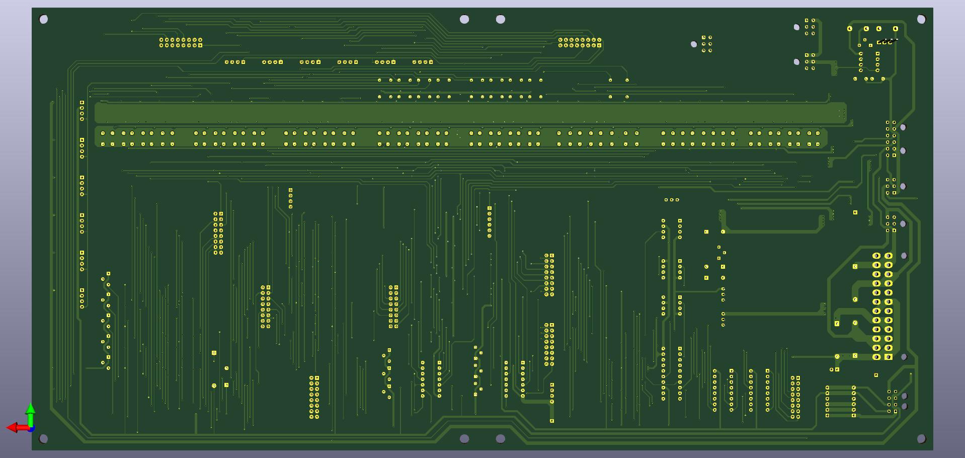
After some consideration, I removed the ground plane initally placed in 100% of the bottom layer of the board. Reason for that was the constatation that for this board, pouring a large ground was producing lots of “dead end” ground areas, which may be even worse than no ground plan at all; one GND and one Earth planes were left for the S&H section only. Ideally, the board would have 4 layers, one of them dedicated for ground only, with no traces. However, there is no need for that. Two layers should do the job nicely. Also, decided to change a few ICs from SMD to DIP format should I have to replace a chip. Anyway, this board is pretty much ready for production. Already ordering the components for this board! After the power supply, this should be the next board to get built.